- HOME
- Products
- UV objective lenses
- Objective lenses for mask / wafer inspection
Objective lenses for mask / wafer inspection
Wide field of view・Long working distance and Aberration-free
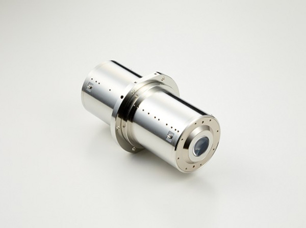
The MI series of objective lenses for mask / wafer inspection have co-functioning with a wide field of view, long working distance and aberration-free, and are suitable for semiconductor photomask / wafer inspection.
Customized support for interface section and various relay lenses is available.
Key features
- Features
-
- From its refractive optical system, it has no shielding , but long working distance.
- It is achromatic within the spectrum of the laser, resulting in good imaging properties.
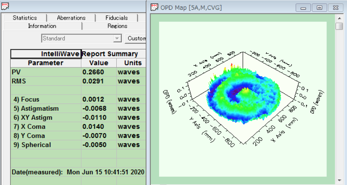
- The design performance is numerically guaranteed by measuring wavefront aberration with an interferometer.
- Suitable for semiconductor mask / wafer observation applications.
- Applications
-
- Semiconductor wafer inspection equipment
- Semiconductor mask inspection equipment
- Sample for an evaluation of transmitted wavefront aberration (MI266-5085)
-
Specification examples
| Model No. | MI193-5085 | MI266-5085 | MI355-5085 |
|---|---|---|---|
| Wavelength | 193.4nm | 266nm | 355nm |
| Bandwidth (full width at half maximum) |
8pm | 5pm | 20pm |
| Type | Refractive type | ||
| Numerical aperture (NA) | 0.85 | ||
| Focal length | 5mm | ||
| Transmittance | ≥ 70% | ≥ 80% | |
| Field of view | Φ0.3mm | Φ0.45mm | |
| Wavefront aberration (monochromatic) |
≤ 0.03 waves rms | ||
| Working distance | ≥ 8mm | ||
| Weight | Approx. 6.5kg | Approx. 7.1kg | Approx. 7kg |
| Operating temperature | 23±0.5℃ | ||
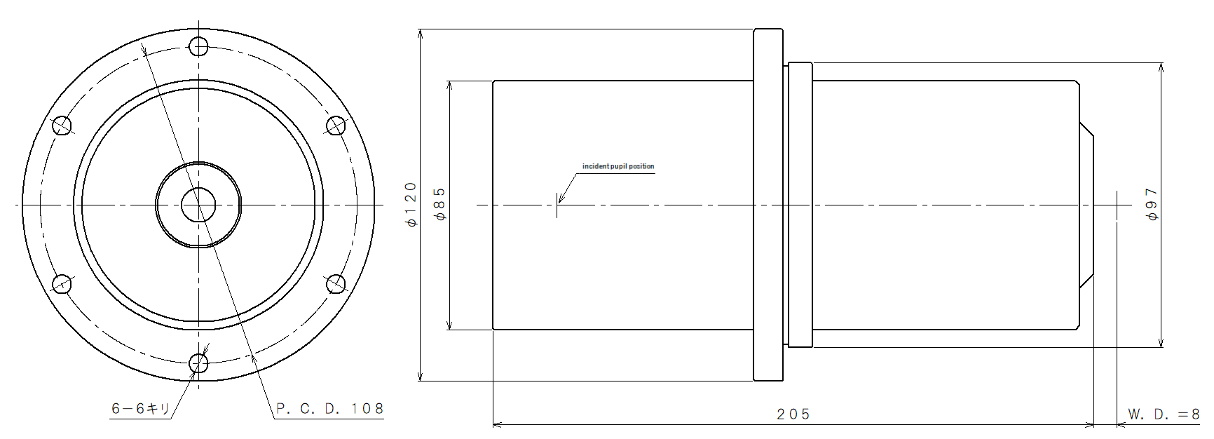
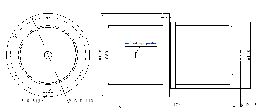
Dimensions
- MI193
-
- MI-266/355
-
Catalog Download

- HOME
- Products
- UV objective lenses
- Objective lenses for mask / wafer inspection